Military and Aerospace: SiOnyx is to develop low-cost "black silicon"-based SWIR imagers for U.S. Naval Surface Warfare Center Dahlgren Division in Dahlgren, Va. Navy researchers say that using the SiOnyx Black Silicon process could increase the IR QE over standard silicon, and lead to a low cost, enhanced SWIR detector.
Thursday, May 31, 2012
Sony Announces HD CMOS Sensors, Promises Stacked Products Soon
Sony Cx-News vol. 68 has few image sensor announcements.
IMX104LQJ CMOS image sensor for industrial applications has 1.37MP resolution and 3.75um pixels. Its frame rate is 120fps at 10b ADC resolution or 60fps at 12b resolution. The sensor is said to provide 12dB higher SNR than existing Sony products. Its low light sensitivity is better, in comparison with IMX035LQR
with slightly smaller 3.63um pixels:
IMX136LQJ (color) and the IMX136LLJ (black and white) industrial CMOS image sensors feature that same 120fps/10b and 60fps/12b speed but at 2.38MP resolution. The pixel size is 2.8um to maintain almost the same 1/3-inch optical format. They also support the multiple frame HDR mode. In this mode, separate
exposure time and gain can be set in advance for 4 or 2 consecutive frames and sets of 4 or 2 frames can be set as a shooting condition to automatically output consecutive images:

Sony also talks more about its image sensor stacking technology: "Sony's Stacked CMOS Image Sensor Solves All Existing Problems in One Stroke".

"Digital still cameras mainly use Type 1/2.3 CMOS image sensors. If the 45 nm process rule can be used for the circuit section, it will become possible to implement signal processing circuits that equal the DSPs used in high-end digital still cameras. And even the 65 nm rule will make possible signal processing for middle class digital still cameras.
Type 1/3.2 image sensor processed according to the 65 nm rule could be incorporated in a surveillance camera. And if the 45 nm rule were used, it would enable integration of a signal processing circuit large enough for middle class digital still cameras.
Secondly, how can the surface area be reduced by completely separating the pixel section from the circuit section?
Sony's Type 1/4 CMOS image sensors can then be reduced by 30% and SoC CMOS image sensors for mobile phones with camera signal processing capability can be reduced by 40%. Although CMOS sensors are generally thought to be larger than CCD image sensors, stacked CMOS image sensors do not need any registers and can therefore be 20% smaller. The configuration of the sensor makes it ideal for use in medical cameras and other industrial applications."
Stacked image sensor products with RGB-W CFA and HDR functions are planned for shipment:
The stacked CMOS image sensor with RGB-W and HDR functions do not require to change the signal processing of the in system, meaning the stacked processor translates output signals to some standard format.

IMX104LQJ CMOS image sensor for industrial applications has 1.37MP resolution and 3.75um pixels. Its frame rate is 120fps at 10b ADC resolution or 60fps at 12b resolution. The sensor is said to provide 12dB higher SNR than existing Sony products. Its low light sensitivity is better, in comparison with IMX035LQR
with slightly smaller 3.63um pixels:
 |
| Low-light Picture Quality (in all-pixel scan and 12-bit A/D conversion mode, 30fps, 0.1 lx, 42dB with built-in PGA +12dB in rear end, at F2.0) |
IMX136LQJ (color) and the IMX136LLJ (black and white) industrial CMOS image sensors feature that same 120fps/10b and 60fps/12b speed but at 2.38MP resolution. The pixel size is 2.8um to maintain almost the same 1/3-inch optical format. They also support the multiple frame HDR mode. In this mode, separate
exposure time and gain can be set in advance for 4 or 2 consecutive frames and sets of 4 or 2 frames can be set as a shooting condition to automatically output consecutive images:

Sony also talks more about its image sensor stacking technology: "Sony's Stacked CMOS Image Sensor Solves All Existing Problems in One Stroke".

"Digital still cameras mainly use Type 1/2.3 CMOS image sensors. If the 45 nm process rule can be used for the circuit section, it will become possible to implement signal processing circuits that equal the DSPs used in high-end digital still cameras. And even the 65 nm rule will make possible signal processing for middle class digital still cameras.
Type 1/3.2 image sensor processed according to the 65 nm rule could be incorporated in a surveillance camera. And if the 45 nm rule were used, it would enable integration of a signal processing circuit large enough for middle class digital still cameras.
Secondly, how can the surface area be reduced by completely separating the pixel section from the circuit section?
Sony's Type 1/4 CMOS image sensors can then be reduced by 30% and SoC CMOS image sensors for mobile phones with camera signal processing capability can be reduced by 40%. Although CMOS sensors are generally thought to be larger than CCD image sensors, stacked CMOS image sensors do not need any registers and can therefore be 20% smaller. The configuration of the sensor makes it ideal for use in medical cameras and other industrial applications."
Stacked image sensor products with RGB-W CFA and HDR functions are planned for shipment:
- Type 1/3.06 stacked CMOS image sensor with approx. 13.0M effective pixels
Sample shipments planned for June, 2012 - Type 1/4 stacked CMOS image sensor with approx. 8.0M effective pixels
Sample shipments planned for August, 2012
The stacked CMOS image sensor with RGB-W and HDR functions do not require to change the signal processing of the in system, meaning the stacked processor translates output signals to some standard format.

Wednesday, May 30, 2012
Omnivision Announces 1.1um OmniBSI-2 12.7MP Sensor, VGA CameraCube
PR Newswire: OmniVision announces the OV12830, a 12.7MP sensor for high-end smartphones and tablets. The 1/3.2-inch OV12830 utilizes 1.1um pixel OmniBSI-2 architecture to capture 1080p/60fps HD video, and full resolution 12MP high-speed photography at 24fps to dramatically reduce shutter lag. The chief ray angle is 30.3deg. non-linear.
"We are bringing this sensor to market at a time when next-generation smartphone and tablet cameras are moving beyond the 8-megapixel threshold," said Devang Patel, senior product marketing manager at OmniVision. "The OV12830 marks OmniVision's highest resolution 1/3.2-inch optical format offering for mobile devices to date, and fits into the industry-standard module size of 8.5 x 8.5 mm."
An on-chip RAW scaler allows the sensor to record video at 30fps while maintaining full field of view. Additionally, the OV12830 is capable of capturing full 1080p/60fps HD video with additional pixels for EIS. The sensor provides alternate row output from full-resolution at two different exposures, enabling HDR still or video recording. The OV12830 comes in die format with 4-lane MIPI interface.
It is currently available for sampling, and is expected to enter volume production in the fourth quarter of 2012.

Another Omnivision's announcement is 1/9-inch VGA CameraCube, the OVM7675, having a
size of 2.9 x 2.9 x 2.3 mm. The CameraCubeChip is built on 2.5um OmniPixel3-HS technology, which delivers sensitivity of 1800 mV/lux-sec. The OVM7675 is currently sampling and is expected to enter volume production in Q4 2012.
Tuesday, May 29, 2012
Omron Announces Gesture Recognition Software for Mobile Apps
Omron announces that it has developed an embedded hand gesture recognition technology capable of simultaneously recognizing the position, shape, and motion of a person's hand or finger by referencing a camera-recorded image. The technology features:
The gesture recognition joins OKAO line of other licenseable image processing routines for mobile applications:

- Trigger motion is not necessary by facial image sensing technology.
- Hand or finger position, shape and movements can be recognized simultaneously.
- Hand gesture detection ranges from very near (about 10cm) to far (several meters).
- High-speed recognition is enabled on smartphones and tablets.
- Small program size makes it possible to embed the technology in a diverse range of devices.
- Recognizable size of hand: 40 pixels or higher
- Recognition start: By hand-waving or automatic via combination of face and hand recognition
- Recognition speed: 30fps at 1.0GHz Snapdragon
- Compatible operating systems: Windows XP/7, Android OS, iOS, etc.
The gesture recognition joins OKAO line of other licenseable image processing routines for mobile applications:

Lfoundry Announces 110nm Process with Imaging Option
PRWeb, EETimes: Rousset, France-based LFoundry announces PDK 110 for ots 110nm Aluminum process. The PDK includes several advanced technology options, especially an embedded Flash which is proposed in 90nm resolution.
"This PDK is particularly well adapted for key applications such as... CMOS imagery," commented Jean-Pierre Delesse, President, LFoundry Rousset. It's not clear if flash memory processing module can be combined with the CIS one.
LFoundry Rousset is a former Atmel fab sold to Germany LFoundry GmbH in 2009. The German LFoundry fab was shut down in 2011.
Digitimes: Omnivision Expands TSMC, Testing Houses Orders
Digitimes: Taiwan packaging and testing houses King Yuan Electronics (KYEC) and Tong Hsing Electronic Industries reportedly have landed new orders for CMOS sensors from OmniVision, with shipments slated to kick off in Q3 2012, according to newspaper's sources.
KYEC and Tong Hsing both said they do not comment on customer status and orders.
OmniVision is believed to have secured orders for Apple's next-generation iPhone and iPad series. KYEC and Tong Hsing previously cut into the supply chain for Apple's iPhone 4S through supplying services to OmniVision, Digitimes' sources report (probably for VGA front camera). Also, OmniVision's wafer starts at TSMC for the second quarter are expected to jump significantly from the prior quarter's levels, the sources pointed out.
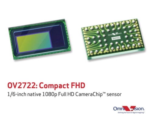
Omnivision Announces 1/6-inch Native 1080p OmniBSI+ Sensor
PR Newswire: OmniVision announces the OV2722, the second-generation native 1080p CMOS sensor, designed for ultra-portable applications such as smartphone, tablet and Ultrabook. Based on 1.4um OmniBSI+ pixel, the OV2722 can be housed in a module height of less than 3 mm. The 1.4um OmniBSI+ pixel offers significant performance improvements over the first generation OmniBSI, including a 60% increase in full-well capacity, a 10% increase in QE and a 10% improvement in low-light performance.
The OV2722 is currently in volume production.

Update: Digitimes reports that ultrabooks will require camera modules height be reduced to 2.0-3.0mm which is lower than 4.0-5.0mm specified for regular notebooks. This will prevent ASPs for webcams from falling in 2012, according to the newspaper's sources.
The OV2722 is currently in volume production.
Update: Digitimes reports that ultrabooks will require camera modules height be reduced to 2.0-3.0mm which is lower than 4.0-5.0mm specified for regular notebooks. This will prevent ASPs for webcams from falling in 2012, according to the newspaper's sources.
Monday, May 28, 2012
Friday, May 25, 2012
Brandywine's 1 Gigapixel Hyperspectral CMOS Sensor
It was brought to my attention that Brandywine Photonics sells a special sensor said to be optimized for multispectral imaging, the FBX-2. The sensor has a number of interesting features. While the main version has 2056 x 256 resolution with 15um pixel pitch, it's said to be available in HDTV, 25MP, 1 GigaPixel(!), and butt-able array formats. The broad spectrum QE looks very good, especially 30% at 1000nm:
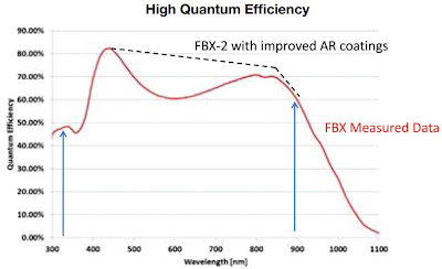
The read noise is said to be <10e-, and the "well depth" is 300K (not sure what are the units of this one).
Thanks to OSP for the link!

The read noise is said to be <10e-, and the "well depth" is 300K (not sure what are the units of this one).
Thanks to OSP for the link!
Engadget Tests Leap Motion Gesture Recognition Device
Engadget published an interview with David Holz and Michael Buckwald, the two men behind Leap Motion's gesture recognition device. While David and Michael refused to explain how it works, they only mentioned it's based on IR LEDs and cameras. The demo looks nice, albeit the window curtain is too dense for my taste:
NHK 33MP/120fps SHV Sensor
First presented at ISSCC 2012, NHK and Shizuoka University Ultra High Definition imaging setup features in quite a few marketing materials this week:
First, the new Super Hi-Vision sensor features on the first page on NHK's Broadcast Technology Bulletin. The article mostly re-iterates the stuff presented at ISSCC.
Second, DigiInfo.tv runs an article accompanied by Youtube video from NHK Open House 2012. The article says that NHK plans to increase the light sensitivity of the 1.5-inch SHV sensor.
Third, the new sensor presentation opens NHK R&D lectures at the company's Open House being held on May 24-27, 2012 in Tokyo, Japan. And there is a dedicated booth showing the new image sensor.
Failure Mechanism in CCD
Truesense patent US8,184,186 talks about an interesting failure mechanism in CCDs:
"A voltage applied to the substrate is set to a first level when the photosensitive regions accumulate charge. When an electronic shutter operation is to be performed, the voltage is changed to a second level. An image sensor, such as an interline charge-coupled device (CCD) image sensor, can be permanently damaged when the image sensor is exposed to extremely bright light during an electronic shutter operation. The damage is caused by a parasitic bipolar transistor formed within the image sensor. FIG. 1 is a schematic of a parasitic bipolar transistor formed in a prior art interline CCD image sensor. An n-type vertical CCD channel can become an emitter of the transistor (Vccd), a grounded p-well under the vertical CCD the base, and an n-type substrate the collector of the transistor (Vsub)."

"At the center of a pixel array the p-well resistance (represented by R in FIG. 1) is very large because the ground contacts are at the edges of the pixel array. This large resistance allows the bright light to generate photocurrent at the base of the transistor faster than the resistor R can drain it away. A bright spot from the sun, for example, can raise the voltage of the base high enough to turn on the transistor and short the electronic shutter voltage to the vertical CCD channel. The high voltage on the vertical CCD channel will inject charge into the vertical CCD gate dielectric. The injected charge first causes increased dark current in the vertical CCD. With continued bright light exposure during multiple electronic shutter pulses, a sufficient amount of charge is injected into the gate dielectric to cause poor charge transfer and image lag."
Truesense's patent proposes to detect the excessive current and block the shutter operation if it exceeds a certain threshold level.
Thursday, May 24, 2012
UMC Develops BSI CIS Process on 12-inch Wafers
UMC CEO Shih-Wei Sun said at groundbreaking ceremony for its 300mm Fab 12A (Phase 5 & 6) at Tainan, south Taiwan fab complex: "UMC... cooperates closely with customers on 300mm specialty technologies such as... BSI CMOS image sensor... and 3D IC TSV to provide a truly comprehensive, leading foundry technology platform".
Nemotek-Tessera WLC Reverse Engineered
Systemplus published reverse engineering report of Nemotek WLC featuring Tessera technology. The wafer-level packaging of the CIS uses Shellcase MVP process with TSVs to connect the bond pads on the die and the BGA interface on the rear face of the package. The wafer-level optics is a single lens
element, reflow compatible, manufactured in OptiML WL-Optics process. The wafer-level camera is entirely assembled by Nemotek Technologie in Morocco.

Meanwhile Tessera-DOC published a nice promotional video on Dropbox (no embedding allowed).
element, reflow compatible, manufactured in OptiML WL-Optics process. The wafer-level camera is entirely assembled by Nemotek Technologie in Morocco.

Meanwhile Tessera-DOC published a nice promotional video on Dropbox (no embedding allowed).
Wednesday, May 23, 2012
Chipworks Survey of Recent Image Sensor Pixel Structures
Chipworks published a nice review of recent FSI and BSI pixel implementations by Ray Fontaine. I was particularly impressed by the recent Foveon-Sigma SD1 Merill pixel managing to squeeze 6T 3-color pixel in 5um pitch:
 |
| Foveon 15.3 Mp x 3 CIS from Sigma SD1 – Pixel Cross Section SCM, Planar View of Pixel at Poly |
Details of Caltech Suit Against RIM, ST, Nokia
Justia web site published details of JPL-Caltech suit against STMicro sensors used in RIM and Nokia camera phones. Honestly, I have not read the long documents that Justia kindly presents on its page, but the lawsuit talks about 6 different ST's sensors allegedly infringing on 6 Caltech patents.
TSR Market Share Data for 2H 2011
Caltech lawyers published market shares data that apparently came from one of the most solid sources - TSR's 2H 2011 report:

There are also few comments on the market and projections for 2012:
"In the 2011 image sensor market in terms of total revenues, Sony secured the largest share of 37.3%. Sony commanded the top share in the CCD area image sensor market and, also in the CMOS area image sensor market, it sold primarily high-end DSLR/mirrorless cameras, high-end camcorders and 8-Mpixel camera phones. It achieved the highest market share in terms of revenue because it sold products of high unit prices. Canon took the second place, followed by Samsung and OmniVision. Canon is increasing its market share in the DSLR application by 43% compared to 2010. Since its unit price zone for DSLR sensors is $65 to 120, Canon is way up on the high level based on the revenue share.
Our projection for 2012 is that Sony will increase its market share and maintain the top position. Its shipments of 1351 sensors for DSCs and camera phones are significantly increasing. Canon plans to ship 10 million DSLRs annually, which is an increase of 33% compared to 2011, and its share of the sensor market in terms of revenue will also increase further, Aptina is also projected to increase shipments of mirror-less camera sensors for Nikon, which will contribute to an increase of its revenue."
Tuesday, May 22, 2012
Toshiba Targets DSC Market
Tech-On reports that Toshiba CEO, Norio Sasaki said in his May 17, 2012 Mid-Term Strategy presentation that the company intends to increase its CMOS sensors business profitability by entering the DSC market where it expects to have higher unit prices.
Stanford/UPenn Team Reduces Wires Light Scattering
NanoWerk: Pengyu Fan working in Stanford University Prof. Mark Brongersma's group is the lead author of an ambitiously-named paper published online on May 20th in Nature Photonics journal: "An invisible metal–semiconductor photodetector".
The paper says that if one covers a silicon nanowire by a thin gold plating, it almost stops scattering light due to cancelling of plasomonic dipoles in Si wire and Au plating:

The researchers propose that plasmonically cloaked pixel wiring in image sensors might reduce the cross-talk between neighboring pixels due to a dramatic reduction of light scattering over broad visible spectrum and wide angle of incidence. The gold plating can be substituted for the more common Cu or Al while maintaining the same cloaking efficiency.
Omnivision Announces 16MP/30fps OmniBSI-2 Sensors
PR Newswire: Omnivision announces the OV16820 and OV16825, two 16MP sensors that support 16MP/30fps burst photography and can capture 4K2K video, or Quad Full High Definition (QFHD), at 60fps. Built on the 1.34um OmniBSI-2 pixel, the OV16820 and OV16825 support emerging standards in high-resolution video recording for DSC/DVC markets and the high-end smartphone market, respectively.
The 1/2.3-inch OV16820 and OV16825 sensors are capable of operating in full resolution (4608 x 3456) video at 30fps, 4K2K (3840 x 2160) video at 60fps, and 1080p HD video at 60fps with extra pixels for EIS. Their image processing functions include defective pixel and noise canceling, RAW scaling, image size, frame rate, exposure, gain, cropping and orientation are programmable through the serial camera control bus (SCCB) interface. The sensors have up to 8-lane MIPI and LVDS data outputs.
"It was an industry-wide assumption that smartphones would cut into DSC/DVC sales; but at higher resolutions, we're seeing a very distinct divide between the two markets and both remain strong," said Devang Patel, senior product marketing manager at OmniVision.
The OV16820 is available for sampling in a ceramic land grid array (CLGA) package while the OV16825 will be available in die form (RW/COB). Lens CRA is 8.5deg (non-linear) for DSC/DVC version or 29.7deg (non-linear) for the mobile version. Both sensors are expected to enter volume production by Q4 2012.
 |
| OV16820 |

Nokia 41MP 808 Pureview Team Presentation
Nokia published a Youtube video presenting the design of its 808 model 41MP camera and the team behind it. The video was shot on 808 camera itself:
Thanks to NE for the link!
Thanks to NE for the link!
Monday, May 21, 2012
Leap Motion Announces New Gesture Interface
San Francisco-based Leap Motion announced its new gesture control system, said to be 100-200 times more accurate than all the existing gesture recognition systems. The Leap is claimed to be able to distinguish individual fingers and track movements down to a 1/100th of a millimeter. The 3D interaction space is limited by 8 cubic feet. The Leap system retail price is going to be $70.
There is now word on the Leap operating principle. The company's Yutube video demos the new system is action:
The initial technology ideas came from Leap Motion's co-founder and CTO David Holz. David was working on a PhD in mathematics from UNC Chapel Hill and left to pursue Leap Motion. Before that, he was conducting research for NASA on fluid mechanics.
CNET publishes an interview with Leap's CEO Michael Buckwald. Leap Motion announced $12.75M in Series A funding led by Andy Miller of Highland Capital Partners earlier this month.
Leap intends to create an ecosystem with a large number of third-party applications, as opposed to trying to build and popularize those apps itself. "We want to create as vibrant a developer ecosystem as possible, and we're reaching out to developers in all sorts of" fields, CEO Michael Buckwald told CNET. Leap Motion is looking for a few hundred developers, but intends to expand the program by sending out between 15,000 and 20,000 free developer kits.
Thanks to CM for the info!
Tessera DOC Publishes MEMS AF Actuator Flyer
Tessera Digital Optics Corp. published its MEMS AF flyer having nice feature list and pictures:
Another DOC flyer presents AF+shutter actuator, where the shutter design appears like mechanical style:

It's said to be fitting to 8.5 x 8.5 x 6mm camera module and has 1M cycles life time.
- Fits in 6.5 mm x 6.5 mm x < 6.0 mm camera module size
- Supports image resolution ≥5 MP
- Centered optical aperture for centered optics
- Supports 1/4” and 1/3” optical formats
- Low operating voltage (2.8 to 4.5 V)
- Zero power consumption at the infinity position to hold focus in any orientation
- Low peak current (7 µA peak) and low power (0.25 mW maximum) to change focus position
- Positioning repeatability: ± 3 µm
- Hysteresis performance: ± 3 µm
- Built-in high precision position sensor for autofocus calibration
- Fast settling time: ≤15ms max
- Long lifetime: 10,000,000 cycles or more
- High shock tolerance: 10,000 g
- Temperature Range: -20º to 70º C
- Reflow compatible
 |
| MEMS AF Actuator |
 |
| Example of a camera module with integrated MEMS AF |
Another DOC flyer presents AF+shutter actuator, where the shutter design appears like mechanical style:

It's said to be fitting to 8.5 x 8.5 x 6mm camera module and has 1M cycles life time.
Saturday, May 19, 2012
Spectral Instruments Offers 112MP CCD Camera
Tucson, AZ-bases Spectral Instruments shows its new product - 112MP CCD camera with 95mm x 95mm B&W sensor. The CCD is cooled down to -100C to reduce noise. The company's Youtube video demos the new 1110s camera:
Spectral Instruments also has 900 series 256MB camera, but the CCD sensor there is composed of 16 lower resolution CCDs.
Spectral Instruments also has 900 series 256MB camera, but the CCD sensor there is composed of 16 lower resolution CCDs.
Thursday, May 17, 2012
Panavision BSI Sensor QE
FastVision published datasheet of its recently announced FC300 camera featuring Panavision 3.2MP/180fps sensor with optional JPL BSI processing. White its peak QE is a respectable 60%, the whole spectral graph looks quite interesting:


Wednesday, May 16, 2012
ESPROS Announces 3D ToF Imager
Swiss ESPROS Photonics Corp. image sensor fab has a number of standard products. Its May 2012 "Chips" magazine (distributed by email) features its latest 3D TOF product, the epc600. Beat De Coi, ESPROS CEO, says:
"Our 3D camera technology is really taking off. All our our customers who have seen the epc600 live in action are excited by this new system. A complete 3D camera measuring only 20×25×30mm! Distance measurements up to 10 meters within milliseconds in bright sunlight conditions. A system developers dream has become true! The new epc600 chip will become available soon, together with a simple to use evaluation kit."
Beat continues: "Agreed, I am really talking it up. But I am still surprised myself how much power is in this tiny device. For three decades, I have been a developer of sensors for industrial applications in the textile industry, automation technology, in elevators, logistics, and many more. How I wish I had such a technology available for my work during these years. We had so many ideas for innovative sensor solutions. But with the technologies available at the time there was simply no way to realize these ideas in commercially viable products. However, with epc things have now changed!"
ESPROS web site says that the new ToF imager has resolution of 8x8 pixels, on-chip LED driver and a range up to 7.5m. The imager is highly integrated and capable to operate under ambient illumination of 10,000 lux.
The magazine also talks about the new ESPROS backside processing line: "This year, we started with the project work for our backside processing line in Sargans. Our ESPROS Photonic CMOS process relies on highly specific semiconductor manufacturing steps that are unique in the open market. A good part of the “secret ingredients” are applied during
the later steps of the silicon manufacturing process, the so called backside processing. As these steps are highly specific and constitute an important part of our technical USP,
it was a strategic decision to implement these production steps into our headquarter's manufacturing portfolio. By end of 2011 the necessary tools were delivered to Sargans and the project was officially started in January 2012. During the course of this year we will install and ramp up this line."
Thanks to OSP for the info!
"Our 3D camera technology is really taking off. All our our customers who have seen the epc600 live in action are excited by this new system. A complete 3D camera measuring only 20×25×30mm! Distance measurements up to 10 meters within milliseconds in bright sunlight conditions. A system developers dream has become true! The new epc600 chip will become available soon, together with a simple to use evaluation kit."
Beat continues: "Agreed, I am really talking it up. But I am still surprised myself how much power is in this tiny device. For three decades, I have been a developer of sensors for industrial applications in the textile industry, automation technology, in elevators, logistics, and many more. How I wish I had such a technology available for my work during these years. We had so many ideas for innovative sensor solutions. But with the technologies available at the time there was simply no way to realize these ideas in commercially viable products. However, with epc things have now changed!"
ESPROS web site says that the new ToF imager has resolution of 8x8 pixels, on-chip LED driver and a range up to 7.5m. The imager is highly integrated and capable to operate under ambient illumination of 10,000 lux.
 |
| epc601 integrated TOF Imager |
The magazine also talks about the new ESPROS backside processing line: "This year, we started with the project work for our backside processing line in Sargans. Our ESPROS Photonic CMOS process relies on highly specific semiconductor manufacturing steps that are unique in the open market. A good part of the “secret ingredients” are applied during
the later steps of the silicon manufacturing process, the so called backside processing. As these steps are highly specific and constitute an important part of our technical USP,
it was a strategic decision to implement these production steps into our headquarter's manufacturing portfolio. By end of 2011 the necessary tools were delivered to Sargans and the project was officially started in January 2012. During the course of this year we will install and ramp up this line."
 |
| ESPROS fab is located deep inside Gonzen Mountain for vibration-free environment |
Thanks to OSP for the info!
Truesense Imaging Launches New Web Site and Blog
Truesense Imaging, former Kodak Image Sensor Solutions, launches its own independent web site featuring a brand-new imaging blog.
Thanks to MDL for the info!
Thanks to MDL for the info!
Monday, May 14, 2012
SMIC Qualified 1.75um Pixels, Reports Strong CIS Process Demand
SMIC's 2011 annual report says "In the CMOS image sensor process technology area, 1.75um pixel device was successfully developed and qualified, and ready for 2 mega and 3 mega pixel applications."
Seeking Alpha: In Q1 2012 earnings call transcript: "Fab specific, our Shanghai 8-inch aluminum fab loading is also strong. Not only driven by powered [inaudible] IC, CMOS image sensor in embedded EE. We have successfully transferred the CMOS image sensor in the embedded EE for our Shanghai 8-inch Fab to Tianjin Fab. And time of type capacity enabling such compatible process capability between Tianjin and the Shanghai Fab will better our flexibility in order to accommodate customer demand."
Seeking Alpha: In Q1 2012 earnings call transcript: "Fab specific, our Shanghai 8-inch aluminum fab loading is also strong. Not only driven by powered [inaudible] IC, CMOS image sensor in embedded EE. We have successfully transferred the CMOS image sensor in the embedded EE for our Shanghai 8-inch Fab to Tianjin Fab. And time of type capacity enabling such compatible process capability between Tianjin and the Shanghai Fab will better our flexibility in order to accommodate customer demand."
Friday, May 11, 2012
Good News Predicted for Image Sensor Market
Electronics Weekly: IC Insights predicts sales of CMOS image sensors to grow 8% in 2012 to $6.3bn compared to $5.8bn in 2011, when the market climbed 29% from $4.5bn in 2010. More importantly, the 2011 increase was the first back-to-back annual sales gain for CMOS image sensors since 2006.
CMOS image sensor sales before the downturn registered a record of $4.6bn in 2008. The sales fell 16% in 2009 and declined nearly 14% in 2007.
IC Insights expect the CMOS image sensor market to reach $10.8bn in 2016 – a CAGR of 13% over the next five years compared to a CAGR of just 5% between 2006 and 2011.
Automotive is the fastest growing CMOS image sensor application with sales reaching $1.8bn in 2016, or about 17% of the market’s total dollar volume that year. Camera cellphones will continue to be the largest CMOS image sensor application in 2016 with sales expected to be $5.4bn or 50% of the revenues overall, compared to about $4.2bn or 72% of the total in 2011.
Update: Solid State Technology published a graph on unit volumes and dollar sales of CMOS sensors based on IC Insights data:

IC Insights ranking of CMOS sensor vendors in 2011:
CMOS image sensor sales before the downturn registered a record of $4.6bn in 2008. The sales fell 16% in 2009 and declined nearly 14% in 2007.
IC Insights expect the CMOS image sensor market to reach $10.8bn in 2016 – a CAGR of 13% over the next five years compared to a CAGR of just 5% between 2006 and 2011.
Automotive is the fastest growing CMOS image sensor application with sales reaching $1.8bn in 2016, or about 17% of the market’s total dollar volume that year. Camera cellphones will continue to be the largest CMOS image sensor application in 2016 with sales expected to be $5.4bn or 50% of the revenues overall, compared to about $4.2bn or 72% of the total in 2011.
Update: Solid State Technology published a graph on unit volumes and dollar sales of CMOS sensors based on IC Insights data:
IC Insights ranking of CMOS sensor vendors in 2011:
- Omnivision
- Samsung
- Sony
- ST Micro
- Toshiba
- Aptina
e2v Announces 2MP Global Shutter Sensor
e2v announces 2MP EV76C570 sensor joining its industrial CMOS image sensor range. The device retains optical compatibility with the 1.3MP Sapphire sensor that is already in production. A 1/1.8 inch optical format is retained thanks to the reduced pixel size of 4.5µm.
The feature list is shared with the 1.3MP version:
The feature list is shared with the 1.3MP version:
- Both rolling and global shutter configuration with 3000:1 global shutter efficiency
- 60fps at full resolution with 120MHz clock
- 4x separately configurable regions of interest including the possibility to program each window with separate exposure and gain settings
- A histogram embedded in the footer of the image data field for image statistics to reduce the processing overhead for auto exposure/gain algorithms
- A lin/log pixel response mode for HDR image capture
- A 10 Bit parallel output which can be compressed to 8 bits using a multi-slope companding technique.
Thursday, May 10, 2012
Himax Reports Q1 Results
Himax reports its Q1 2012 results. Its CEO, Jordan Wu, says few words about the image sensor business: "In our CMOS image sensor product line, we have successfully penetrated several top-tier customers in the notebook/PC markets with some shipments already started at the end of the first quarter. In 2012, we expect to see significant shipments of our HD720p sensors, which are used by many customers to replace the older VGA sensors with the proliferation of Windows 8. We are also seeing rapid growth and promising opportunities in China for our new sensor products used in both the smartphone and automotive/surveillance product segments."
Sony is Second Sourcing Sensors for Samsung Smartphones
It was brought to my attention that Sony sells sensors not only to iPhone 4S, but also to its main rival - Samsung Galaxy S II. While the initial Chipworks and SystemPlus reverse engineering reports found Samsung's own 8MP 1.4um sensors inside Galaxy S II, the more recent Chipworks report of China Mobile's Samsung Galaxy S II (Model I9108) discovered Sony IMX105PQ inside.
Wednesday, May 09, 2012
Aptina, Omnivision Join Auto Ethernet Alliance
PR Newswire: The OPEN Alliance (One-Pair Ether-Net) Special Interest Group (SIG), established to drive wide-scale adoption of Ethernet-based automotive connectivity announces a membership increase. Aptina and Omnivision are among the 35 new members.
Key to the Open Alliance SIG is the proliferation of Broadcom's BroadR-Reach technology as an open standard. BroadR-Reach delivers high-performance bandwidth of 100Mbps over an unshielded single twisted pair cable. By eliminating the need for expensive shielded cabling, automotive manufacturers can significantly reduce connectivity costs and cabling weight. License to the specification for BroadR-Reach is available to OPEN Alliance members under RAND terms via a license from Broadcom.
To me it sounds like Omnivision and Aptina are going to release sensors or, may be, image processors with Ethernet interface. This might have much broader implications than just automotive sector.
Panavision Announces 1080p/120 5um Global Shutter Pixel Sensor
Panavision Imaging announces Dynamax DYN0021 2.14MP CMOS image sensor, a 2/3-inch 1080p/120 video sensor with more than 130dB DR in either global shutter or rolling shutter mode, aimed at industrial markets. The sensor features:
The sensor's typical power consumption at 60fps speed is less than 760mW.
- Active Column Sensor (ACS) technology, which achieves reduced noise levels at high gain settings,
- Correlated Multi-Sampling (CMS) technology, to further reduce noise or add gain,
- Dual rolling or global shutter integration for intra-frame, on-chip HDR imaging
- Dual words per pixel for dual gain per pixel
The sensor's typical power consumption at 60fps speed is less than 760mW.
Tuesday, May 08, 2012
Toshiba Aims to Increase its Market Share
Toshiba announced its FY2011 results and targets for FY2012. One of the main targets in Electronic Devices business is to "expand its share in CMOS sensor for digital cameras by achieving low power consumption, high image quality sensor technology." The company intends to do it by "increasing the human resources assigned to development."
Meanwhile Toshiba released a new flyer for its 8MP 1.12um pixel T4K05 BSI sensor. It appears to be a production version, as most TBD lines from the preliminary flyer have been deleted.

Meanwhile Toshiba released a new flyer for its 8MP 1.12um pixel T4K05 BSI sensor. It appears to be a production version, as most TBD lines from the preliminary flyer have been deleted.

Monday, May 07, 2012
Panavision 3.2MP BSI Sensor Uses JPL Process
Business Wire: FastVision announced that its FC300 camera is built around the quiet, high speed sensor supplied by Panavision Imaging. "Panavision Imaging now offers one of the quietest CMOS sensor designs in the world," says Dr. Joseph Sgro, CEO of FastVision and its sister company Alacron. "Our new FC300 camera reflects many advantages of this new sensor including low cost and high speed of 3.2 megapixels running at 180 frames per second."
Sgro explains that this technology can be made into a back-side imager (BSI) with delta doping (DD) and anti-reflective (AR) coating. "Our technology development effort over the past several years with Jet Propulsion Laboratory (JPL) incorporates JPL’s patented delta doping process on the sensor in the FC300," Sgro adds. "This combination of JPL’s DD process and Panavision’s extremely quiet CMOS sensor produces 100 percent fill factor and allows selection of the sensor’s sensitivity to specific wave length, ranging from deep ultra-violet (DUV) to near infrared (NIR)."
Sgro explains that this technology can be made into a back-side imager (BSI) with delta doping (DD) and anti-reflective (AR) coating. "Our technology development effort over the past several years with Jet Propulsion Laboratory (JPL) incorporates JPL’s patented delta doping process on the sensor in the FC300," Sgro adds. "This combination of JPL’s DD process and Panavision’s extremely quiet CMOS sensor produces 100 percent fill factor and allows selection of the sensor’s sensitivity to specific wave length, ranging from deep ultra-violet (DUV) to near infrared (NIR)."
CPIQ Becomes IEEE P1858
Business Wire, EETimes: The Camera Phone Image Quality (CPIQ) effort started in 2007 as a project at the International Imaging Industry Association (I3A). The IEEE acquired the project and related assets from I3A and officially re-launched the project in March as IEEE P1858.
"IEEE is the obvious choice to take CPIQ to the next level," said Lisa Walker, president of I3A. "The competency that IEEE has built around assessing mobile-video quality provides an opportunity for an easy transition and expansion of the work to important, related areas such as video."
It’s not yet clear what certification or validation procedures the group may define. However its work is expected to be finished in 18-24 months, said Edward Rashba, an IEEE director of new business ventures. "If engineers can build to a common spec and performance requirements that will be a good outcome," he said.
Human Eyes as an Image Sensor
This is a pretty old 2001 Yoshio Fukui notes, but it's still a best summary of human eye properties expressed in image sensor terms I've seen. Few quotes:
Spectral sensitivity:
Light-adapted eyes: 400 – 700 nm (peak at 555 nm: yellow light)
Dark-adapted eyes: 380 – 650 nm (peak at 507 nm: green light)
QE:
At low luminance = 5%
At high luminance = 0.5%
A slightly expanded version of Yoshio Fukui lecture is here.
Spectral sensitivity:
Light-adapted eyes: 400 – 700 nm (peak at 555 nm: yellow light)
Dark-adapted eyes: 380 – 650 nm (peak at 507 nm: green light)
QE:
At low luminance = 5%
At high luminance = 0.5%
A slightly expanded version of Yoshio Fukui lecture is here.
Sunday, May 06, 2012
Video Stabilization and Rolling Shutter Artifacts Removal on Youtube
Google Research: The next time you upload your videos to YouTube, YouTube will automatically detect if your video needs stabilization and offer to do it for you. Many videos on YouTube have already been enhanced using this technology. More recently, starting from May 4, 2012, Google implemented rolling shutter removal as well. The before and after videos below show the effectiveness of the new Youtube algorithms:
Google's recent paper "Calibration-Free Rolling Shutter Removal" was awarded the best paper at IEEE International Conference on Computational Photography, 2012. The video examples of the paper's algorithm are on Youtube:
Google's recent paper "Calibration-Free Rolling Shutter Removal" was awarded the best paper at IEEE International Conference on Computational Photography, 2012. The video examples of the paper's algorithm are on Youtube:
Kodak ISS Manufacturing Control
Microsoft published "Kodak Case Study" on how Kodak Image Sensor Solutions Group (Truesense now) uses MS SQL Server to control its manufacturing process. Few interesting quotes:
"ISS produces more than 400 different products and must manage specific process flows in fab, assembly and test for each.
The front end operation puts silicon wafers within a lot on a workflow that involves about 300 to 400 steps. This process takes from three to four months to complete. The back end workflow takes the die—the imagers that are on those wafers—and cuts them into individual die or sensors, and then packages them into a product that can be used in any number of devices. This takes about 10 days to two weeks to complete."
"Kodak ISS has a diverse portfolio of products. Even within that product portfolio, there is some variance for each of those products that requires some specification inline to make each perform differently for the end customer."
Friday, May 04, 2012
First Eedoo Reviews: Much Better than Anticipated
Kotaku published the first look review of China's Eedoo competitor of Microsoft Xbox360 console, including the Kinect. Their conclusion is:
"I can say that it was much better than I had anticipated. The motion tracking was for the most part worked, I was expecting much worse. At the same time the system felt too much like a me too system. It looks and feels way too much like the Xbox 360 and Kinect. There wasn’t really much innovation, and so far, I don’t believe it lives up to its 3799RMB ($587) price tag."

Update: Kotaku published the full Eedoo CT510 review. The conclusion is similar "Exceeding all of my wildest expectations by just working, the CT510 is a very impressive first for a no name Chinese company trying to make a name for themselves. Unfortunately for eedoo its 3,799 RMB (600 USD) price tag really kills it."
"I can say that it was much better than I had anticipated. The motion tracking was for the most part worked, I was expecting much worse. At the same time the system felt too much like a me too system. It looks and feels way too much like the Xbox 360 and Kinect. There wasn’t really much innovation, and so far, I don’t believe it lives up to its 3799RMB ($587) price tag."
Update: Kotaku published the full Eedoo CT510 review. The conclusion is similar "Exceeding all of my wildest expectations by just working, the CT510 is a very impressive first for a no name Chinese company trying to make a name for themselves. Unfortunately for eedoo its 3,799 RMB (600 USD) price tag really kills it."
DSLR Rumors: Nikon to Use Aptina Sensor, Leica to Use ST's One
NikonRumors, PetaPixel: Italian website MarsicaLive started the rumor that the next generation entry level Nikon DSLR D600 will use Aptina's sensor, specifically designed for Nikon.
Leica News and Rumors: Meanwhile, French website lesnumeriques.com tells that Leica will be releasing a new medium format SLR camera (S3?) during the Photokina 2012 show. The Leica S3 will feature a new medium format CMOS sensor produced by STMicroelectronics. The same French article says that Microsoft Kinect uses ST-made sensors too (may be second source to Aptina?).
Leica News and Rumors: Meanwhile, French website lesnumeriques.com tells that Leica will be releasing a new medium format SLR camera (S3?) during the Photokina 2012 show. The Leica S3 will feature a new medium format CMOS sensor produced by STMicroelectronics. The same French article says that Microsoft Kinect uses ST-made sensors too (may be second source to Aptina?).
Thursday, May 03, 2012
Caltech Sues ST, Nokia, RIM over Image Sensor Patents Infringement
Law360: The California Institute of Technology accused Nokia, Research In Motion and STMicroelectronic of importing products that allegedly infringe on its patents on image sensing technology.
Caltech asked the U.S. International Trade Commission to launch an investigation into claims that semiconductor manufacturer STM made smartphone camera components that infringe the school's patented technology, then sold the parts to Nokia and RIM for use in Blackberry devices and other phones.
Caltech asked the U.S. International Trade Commission to launch an investigation into claims that semiconductor manufacturer STM made smartphone camera components that infringe the school's patented technology, then sold the parts to Nokia and RIM for use in Blackberry devices and other phones.
15000-pixel Retina Sensors Implanted in the UK
BBC: Oxford Eye Hospital and King's College Hospital in London, UK carry out clinical trials implanting 1,500-pixel sensors into the eyes of two blind patients. When light enters the eye and reaches the 3 sq. mm chip, it stimulates the pixels which sends electronic signals to the optic nerve and from there to the brain. The chip can have its sensitivity altered via an external power unit which connects to the chip via a magnetic disc on the scalp. The implant was developed by a German company, Retina Implant AG. The patients are now able to perceive light and even some shapes.
Thanks to CDM for the link!
Thanks to CDM for the link!
Wednesday, May 02, 2012
TSMC Proposes to Have Color Crosstalk Test Patterns Alongside the Array
TSMC patent application US20120098975 proposes to have color crosstalk calibration patterns alongside the array, so that any color filter, microlens or metal misalignment can be calibrated on per die or per reticle basis:
 |
| Example of calibration pixels location |
 |
| Example of crosstalk test patterns |
Tuesday, May 01, 2012
FPN in Saturation
Albert Theuwissen discusses pixel FPN in saturation in his "How to Measure..." series of posts. The article discusses the root causes of saturation charge variations and the characterization procedures.
Subscribe to:
Posts (Atom)